Table of Contents
DTL- Logic families
Digital integrated circuits (ICs) were designed based on the characteristics of different types of semiconductor devices. Many complex digital functions were developed in different forms, and each form was named a logic family. In this article we will learn about DTL which is a member of bipolar logic families. Click here to read this article in Hindi
Diode Transistor Logic
DTL circuits are more complex than RTL circuits, but this logic has replaced RTL due to its greater FAN OUT capability and improved noise margin. The main drawback of DTL is its slow speed and because of this drawback, modifications were done in DTL and TTL-Transistor Transistor logic was developed. Today TTL is a very popular and powerful logic family and its mechanism of action is very reliable in SSI and MSI. To understand the superiority of TTL-Transistor Transistor logic, we must first understand DTL.
Initially using input diode and a transistor inverter D.T.L. Circuits were created which were later developed as integrated circuits (ICs).

A 3-input DTL NAND gate is shown in the photo. The basic gate of DTL system is a NAND gate. The input diodes DA, DB, DC have conduction through resistance R. The diode conducts only when the input is in LOW state. Diodes remain in non-conducting state when the input is high. So if one of the inputs is in LOW state then the diode connected to this input will be in forward bias and conduct in it. The voltage generated at point P keeps the transistor T in cut off, so the output of the circuit will be equal to Vcc i.e. HIGH.
On the contrary, if all the three inputs are in HIGH state, then the input diodes DA, DB and DC will be cut off and current will flow from the supply Vcc through resistance R which will lead the transistor to saturation and the output of the circuit will go LOW. This LOW level of the output will be equal to VCE(sat).
DTL AND & OR gate
In the photo below, DTL AND gate is shown on the left side and DTL OR gate is shown on the right side of the photo. In both the circuits, the logic states 1 and 0 are taken as positive logic +5V and 0V respectively.
and in DTL AND circuit (left side) when any input (A1, A2 or A3) is at low logic (0) then diode connected to that input is in forward bias then transistor T comes in cut off. And the output is LOW (logic 0). If all inputs are at logic 1(+5V) then none of the diodes conduct and transistor T conducts heavily. The transistor saturates and the output is HIGH (logic 1).
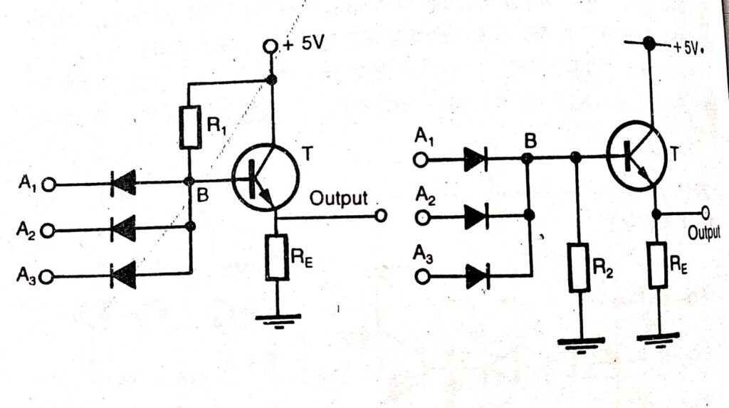


The DTL OR gate is shown on the right side of the photo. If any of the inputs is at logic 1 (+5V) then the diode connected to it conducts and the base (point B) of the transistor is at +5V. Due to excessive conduction in the transistor, it saturates and the output becomes HIGH (logic 1). If all the inputs are at ground level (logic 0) then none of the diodes will conduct and the voltage at point B will be 0. As a result the transistor will be cut off and the output will be LOW (logic 0).
DTL Parameters
- FAN Out – 8
- Noise margin- 0.7 volts
- Propagation Delay- 30n sec
- Power Dissipation -60mW
- Power Supply Voltage(Vcc)- +5 V
Advantages and Disadvantages of DTL
D.T.L. circuits have faster switching speed than RTL circuits because the signal flow into the transistor is through the low resistance of the forward biased diode. Due to the combination of gates in DTL circuit being in 1 state, the input impedance is high so the number of FAN OUT can be increased . The use of diodes in place of resistors and capacitors in DTL circuits makes them cheaper as ICs because diode fabrication on ICs is simpler than resistors and capacitors. Power loss in DTL circuits is low.
D.T.L. The main drawbacks of the circuits are their poor noise margin and low operating speed.
You may read following articles also..
- Digital Integrated Circuit | What is an ICs?
- Control Wiring | Control Panel Wiring | Star Delta Power Wiring | Power wiring
- Wiring diagram | house wiring diagram | staircase wiring diagram
- What is Parity ? | Parity Checker and Generation
- Number System | Types, Conversion rules & Examples