Table of Contents
What are the logic gates ?
In this article-what is Logic gates , we will discuss different types of gates, their symbols, operation etc. Logic gates are based on Boolean algebra. Boolean algebra is a mathematical logic system and it is different from normal algebra and binary number system. For example, in Boolean algebra, 1+1 = 1. In the Boolean system, only two states of the variables are true or false. These are often represented by 0 and 1. The main Boolean operations are AND, OR and NOT. Boolean variable quantities can also be represented by the ON or OFF state of electronic switching circuits. The laws of Boolean algebra are implemented with the help of electronic switches, which are called electronic logic circuits. Click here to Read this article in Hindi
Thus in the Boolean system there are only two quantities 0 and 1. Every number is either 0 or 1. There are no negative or fractional numbers in this system. We can say that if a number X=1 then X ≠0. Similarly if X= 0 then X≠1.
AND gate | AND Logic Gates
An electric switch can be used to represent an AND gate. In the photo below two switches A and B are connected in series. The lamp will illuminate only when both the switches A and B are close. In the first figure, the symbol used in electronics for AND gate is displayed.


AND logic gates operation
The operation is represented by AND symbol (·). Its operation can be written as follows.
A AND B = A·B = Y
This statement means that if A is true and B is true then Y is also true. In any other case Y will be false. There can be four different combinations of A and B as shown in the truth table below. A table in which all possible conditions are tested and it is decided whether the output will be true or false is called truth table. It is known from the truth table that when both A and B are 1 means true then only the output will be Y = 1 means true.
AND logic gates truth table | Truth Table of AND gate
Truth table of AND gate is as below-
| Inputs | Output | |
| A | B | Y=AB |
| LOW | LOW | LOW |
| LOW | HIGH | LOW |
| HIGH | LOW | LOW |
| HIGH | HIGH | HIGH |
| Inputs | Output | |
| A | B | Y=AB |
| 0 | 0 | 0 |
| 0 | 1 | 0 |
| 1 | 0 | 0 |
| 1 | 1 | 1 |
AND gates circuit & operation
A diode AND circuit is shown in the photo below. This type of circuit has more than one input. In this the output is obtained only when the signal is given to all the three inputs simultaneously. For this reason such a circuit is called AND circuit. It is also called coincidence circuit. When there is no signal at any of the inputs, the diodes will be in forward bias and will conduct excessively. Due to the low resistance of the diode, high load resistance RL and low source impedance, this circuit will act as a clamper and the output will be clamped almost to ground level (0).
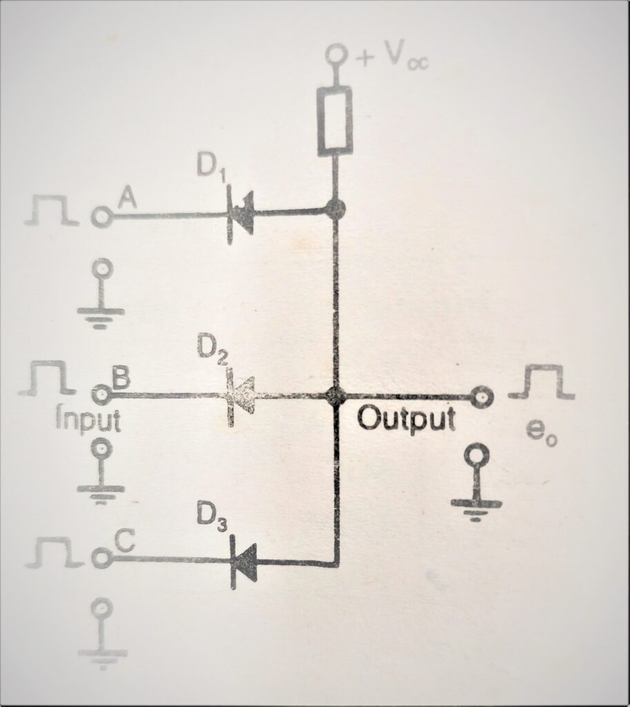
When a positive going pulse is applied to any input (let A) then its amplitude exceeds the power supply +VCC and reverse biases the diode D1. Hence this diode will not conduct. But D2 and D3 diodes (which do not have input signals) are still conducting heavily, so they keep the output at ground level (0). If the inputs are given at A and B and not at C then the output remains at zero level (0) due to conduction in D3. Therefore, the output from this circuit is possible only when the input pulse is given to all the three inputs A, B and C simultaneously.
OR gate | OR Logic Gates
The symbol of OR gate used in electronics circuits is shown in photo (a) below, and its electrical equivalent circuit is shown in second photo (b) of logic gate.


OR Logic gates operation
OR gate operation is shown by the sign (+). OR gate operation can be represented as follows –
A OR B=A+B=Y
This means that if A is true and B is true then Y is also true.
OR gate truth table | Truth table of OR logic gates
There are four different combinations of A and B that can be made. The table below shows the output Y corresponding to different combinations of A and B. It is known from the truth table that if either A or B is true (1), then the value of output Y is true (1).
| Inputs | Output | |
| A | B | Y=A+B |
| 0 | 0 | 0 |
| 0 | 1 | 1 |
| 1 | 0 | 1 |
| 1 | 1 | 1 |
OR gate circuit & Operation
The diode circuit for an OR logic gate is shown in the photo below. A circuit may have two or more inputs. This circuit gives output when signal is given on any one or all the inputs. If all the inputs in the circuit are at zero level (0) then there will be no conduction in any of the diodes. The current in RL will be zero and the output will be zero.

When a positive pulse is applied to any of the inputs (A , B or C ), a current flows through RL due to the corresponding diode being forward biased and a voltage drop across it, which is the output of the circuit. Since the value of RL is much greater than the forward resistance of the diode, the output is approximately equal to the input. Therefore, due to the maximum value of the output, there is no special effect on the output if there is conduction in other diodes. The output of the circuit is same when there is conduction in one diode or all the diodes.
Inclusive OR gate
The above described OR gate in which the output Y = 1, when both the inputs A = 1 and B = 1, is called Inclusive OR gate.
Exclusive OR gate
In this gate, the output Y is true only when either input A or input B is true, not both. The symbol and truth table of Exclusive OR gate are shown in the photo below.

| Inputs | Output | |
| A | B | Y=A+B |
| 0 | 0 | 0 |
| 0 | 1 | 1 |
| 1 | 0 | 1 |
| 1 | 1 | 0 |
NOT gate
The operation of NOT gate is represented by putting a bar like Ā. Operation NOT is also called complementation, negation or inversion. Hence NOT gate is called complementary circuit or inverter. This gate has only one input and one output. The NOT gate inverts or complements the input.
NOT gate truth table | Truth table of NOT gate
In NOT logic gate if the state of the input is 1 then the state of the output will be 0 and if the state of the input is 0 then the state of the output will be 1. The truth table of NOT gate is as follows.
| Input(A) | Output(Y=Ā) |
| 1 | 0 |
| 0 | 1 |
NOT logic gates operation
As mentioned above, NOT logic gate is also called complementary circuit or inverter, it inverts or complements the gate input. If the input of NOT gate is 1 then the output will be 0 and if the input is 0 then the output will be 1. In the photo below (a) the symbol of NOT gate is shown on the left and in the photo on the right (b) its electrical equivalent circuit is shown. When switch A is closed i.e. in logic state 1 then the bulb does not light up i.e. in state 0 because the closed switch short circuit the lamp. Similarly, when the switch is open (state 0), the bulb glows (state 1).

In the symbol of NOT gate, the symbol of bubble represents inversion and the symbol of triangle represents amplifier. The use of bubble symbol as an inversion is shown in the following photo of logic gate.
Electronic Circuit for NOT operation
A transistor circuit for NOT operation is shown in the photo below. This is a simple common emitter amplifier circuit whose output is 180 degrees out of phase with the input.
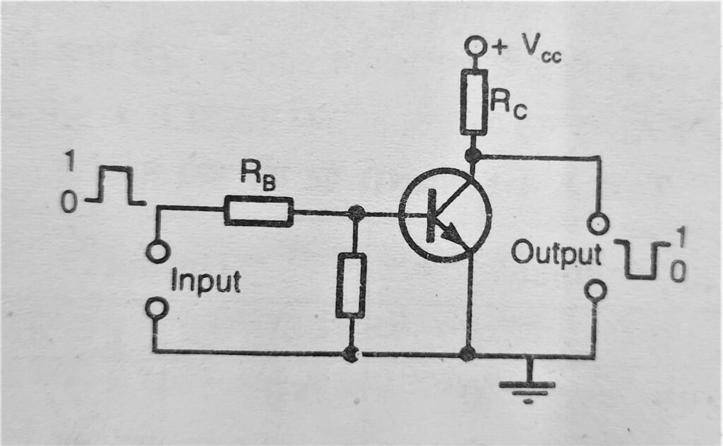
When there is no signal at the input then the collector current is zero (because in this circuit the transistor is biased at cut off) so the output of the circuit is equal to the supply voltage Vcc (state 1). When a positive square wave is applied to the input, the transistor conducts and the collector potential drops to the ground level (state 0). At this time there is no output of the circuit.
Thus the output in the circuit is obtained only when the input signal is zero. Hence it is called NOT circuit.
Hope you liked this article “Logic gates”. You are invited for any kind of suggestion or feedback in the comment box. You can also mail us your suggestions or feedback directly at theinstrumentguru@gmail.com. To read more such articles related to Technology, Electronics and Instrumentation. You can also download our Android App. Click here to download the mobile app.
Read also
- Digital Integrated Circuit | What is an ICs?
- Control Wiring | Control Panel Wiring | Star Delta Power Wiring | Power wiring
- Wiring diagram | house wiring diagram | staircase wiring diagram
- What is Parity ? | Parity Checker and Generation
- Number System | Types, Conversion rules & Examples